NTE5700 thru NTE5705
Industrial Power Module
Description:The NTE5700 throygh NTE5705 series of
Integrated Power Circuits consists of power thyristors and power diodes
configured in a single package. Applications include power supplies, control
circuits, and battery chargers.
Features:
- Glass Passivated Junctions for Greater Reliability
- Electrically Isolated Base Plate
- High Dynamic Characteristics
Absolute Maximum Ratings:
Maximum Repetitive Peak Reverse Voltage
(VS </= 0), VRRM |
|
1200V |
Maximum Non-Repetitive Peak Reverse Voltage,
VRSM |
|
1300V |
Maximum Repetitive Peak Off-State Voltage (
ate Open Circuit), VDRM |
|
1200V |
| |
| Thermal and Mechanical Characteristics: |
| Junction Operating Temperature Range, TJ |
|
-40° to +125°C |
| Storage Temperature Range, Tstg |
|
-40° to +150°C |
Maximum Internal Thermal Resistance,
One Junction-to-Case, RthJC |
|
|
| DC
Operation |
|
2.24K/W |
| Maximum Thermal Resistance, Base-to-Heatsink, RthCS |
|
|
| Mounting
Surface Smooth and Greased |
|
0.10K/W |
| Mounting Torque, Base-to-Heatsink ±10% (Note 1), T |
|
5Nm |
| Approximate Weight, wt |
|
58g (2oz) |
| Note 1. |
A mounting compound is recommended and the torque should
be checked after a period of about 3 hours to allow for the spread of the
compound. |
Electrical Characteristics:
Click on the Part Number for Pricing.
Click on the  for Detailed Acrobat PDF Specifications. for Detailed Acrobat PDF Specifications.
| Parameter |
Symbol |
Test Conditions |
Rating |
Unit |
| Forward Condition |
| Maximum DC Output Current |
IO |
TC = +85°C, Full Bridge
Circuits
(NTE5700, NTE5701, NTE5702) |
25 |
A |
| Maximum Average ON-State Current |
IT(AV) |
180° Sine Wave Conduction
Circuits
(All Types) |
12.5 |
A |
| Maximum Average Forward Current |
IF(AV) |
12.5 |
A |
| Maximum RMS Current |
IRMS |
180° Sine Wave Conduction Circuit
(NTE5702 Only) |
28 |
A |
| Maximum Peak, One-Cycle
Non-Repetitive On-State or Forward Current |
ITSM
or
IFSM |
10ms |
100% VRRM
Reapplied |
Sinusoidal Half Wave, Initial
TJ = TJ Max |
300 |
A |
| 8.3ms |
315 |
A |
| 10ms |
No Voltage Reapplied |
357 |
A |
| 8.3ms |
375 |
A |
| Maximum I2t for
Fusing |
I2t |
10ms |
100% VRRM
Reapplied |
Initial TJ =
TJ Max |
450 |
A2s |
| 8.3ms |
410 |
A2s |
| 10ms |
No Voltage Reapplied |
637 |
A2s |
| 8.3ms |
580 |
A2s |
| Maximum Value of Threshold Voltage |
VT(TO) |
TJ = +125°C |
0.82 |
V |
| Maximum Value of On-State Slope
Resistance |
rT |
TJ = +125°C |
12 |
m Ohm |
| Maximum Peak On-State Voltage |
VTM |
ITM = 3.14 x
IT(AV) |
TJ = +25°C, 108°
Condition |
1.35 |
V |
| Maximum Peak Forward Voltage |
VFM |
IFM = 3.14 x
IT(AV) |
1.35 |
V |
| Maximum Non-Repetitive Rate-of-Rise of Turned
On Circuit |
di/dt |
TJ = +125°C, from
0.67VDRM, ITM = 3.14 x IT(AV),
Ig = 500mA, tr < 0.5µs, tp >
6µs |
200 |
A / µs |
| Maximum Holding Current |
IH |
TJ = +25°C, Anode Supply
= 6V, Resistive Load, Gate Open Circuit |
100 |
mA |
| Maximum Latching Current |
IL |
TJ = +25°C, Anode Supply
= 6V, Resistive Load |
250 |
mA |
| Triggering |
| Maximum Peak Gate Power |
PGM |
|
8 |
W |
| Maximum Average Gate Power |
PG(AV) |
|
2 |
W |
| Maximum Peak Gate Current |
IGM |
|
2 |
A |
| Maximum Peak Negative Gate Voltage |
-VGM |
|
10 |
V |
| Maximum Gate Voltage Required to
Trigger |
VGT |
TJ = -40°C |
Anode Supply = 6V, Resistive
Load |
3 |
V |
| TJ = +25°C |
2 |
V |
| TJ = +125°C |
1 |
V |
| Maximum Gate Current Required to
Trigger |
IGT |
TJ = -40°C |
Anode Supply = 6V, Resistive
Load |
90 |
mA |
| TJ = +25°C |
60 |
mA |
| TJ = +125°C |
35 |
mA |
| Maximum Gate Voltage that will not
Trigger |
VGD |
TJ = +125°C, Rated
VDRM Applied |
0.2 |
V |
| Blocking |
| Maximum Critical Rate-of-Rise of Off-State
Voltage |
dv / dt |
TJ = +125°C, Exponential
to 0.67VDRM, Gate Open Circuit |
200 |
V / µs |
| Maximum Peak Reverse Leakage Current at
VRRM |
IRM |
TJ =
TJ Max, Gate Open Circuit |
10 |
mA |
| Maximum Off-State Leakage Current at
VDRM |
IDM |
2 |
mA |
| RMS Isolation Voltage |
VINS |
50Hz, Circuit-to-Base, All
Terminals Shorted |
2500 |
V |
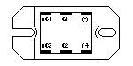
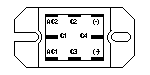
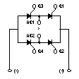
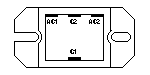
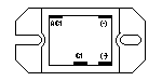
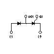
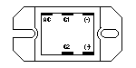
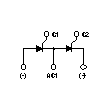
Pin Connection and Schematic Diagrams: (* For
transient protection, a Metal Oxide Varistor (MOV) may be connected
externally across terminals AC1 & AC2.)
| NTE No. |
Description |
Terminal Positions |
Schematic Diagrams |
| 5700 |
Single Phase,
Hybrid Bridge,
Common
Cathode,
Freewheeling Diode |
 |
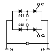 |
| NTE5701 |
Single Phase,
Hybrid Bridge,
Common
Anode,
Freewheeling Diode |
|
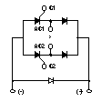 |
| NTE5702 |
Single Phase,
All SCR Bridge |
 |
 |
| NTE5703 |
SCR AC Switch |
 |
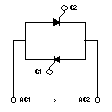 |
| NTE5704 |
Hybrid Doubler |
 |
 |
| NTE5705 |
SCR Doubler |
 |
 |
|